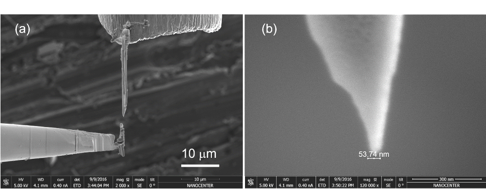
Attachment of a W5O14 nanowires to the ion cut W-wire using FIB manipulator.
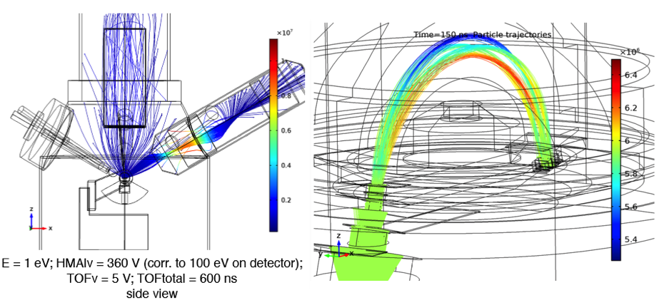
Simulated trajectories within the analysis chamber and the HMA analyzer (the color bar represents the velocity [m/s] of the particles in the fields).
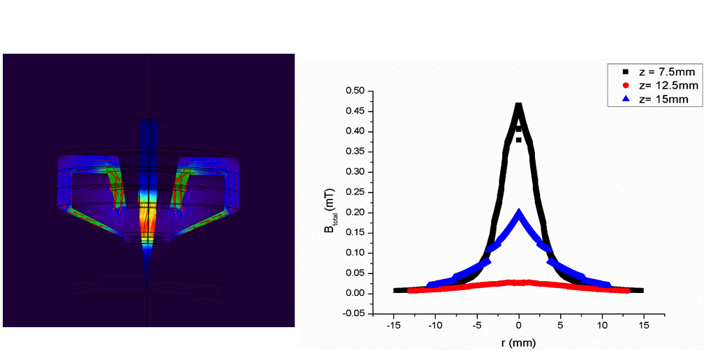
Simulation of SEM objective Lens: magnetic field distribution of a SEM objective Lens is cylindrically symmetric.
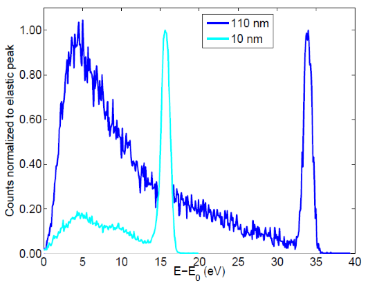
Energy spectra of secondary electrons backscattered from a cleaved GaAs(110) surface for two different tip-sample distances of 10 and 100 nm, acquired at the same spot.
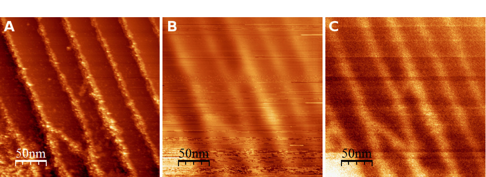
Images of a stepped W(110) surface (a) STME-, (b) absorbed current image and
(c) secondary electron image
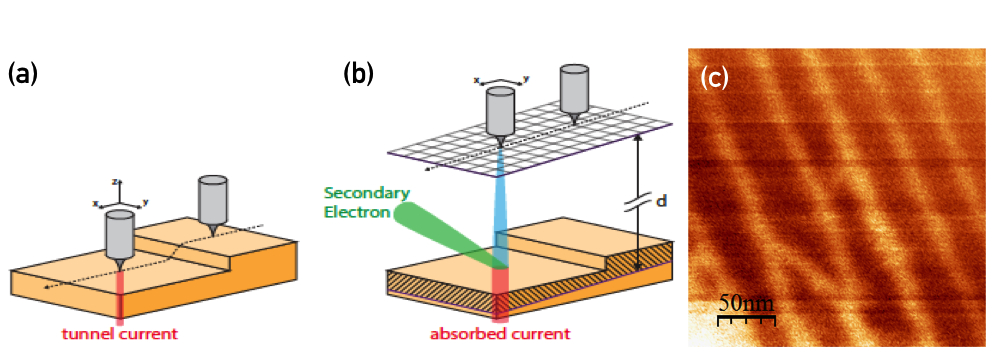
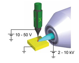
(a) Schematic view of Scanning Tunnelling Microscopy. (b) In NFESEM the tip is retracted to larger tip-target distances.
The SIMDALEE2-consortium during the kick-off meeting on the roof of the Vienna University Technology.
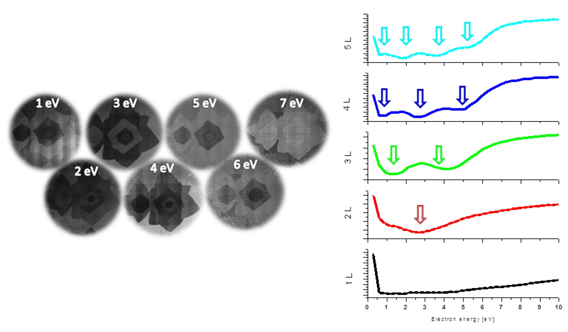
Stack of graphene layers on a copper substrate imaged at extremely low energies, together with energy dependences of the local reflectivity revealing number of stacked layers via number of reflectivity minima.
Ultrahigh-vacuum scanning electron microscope with detection of reflected and transmitted electrons of any energy and analysis of Auger electrons and desorbed ions.
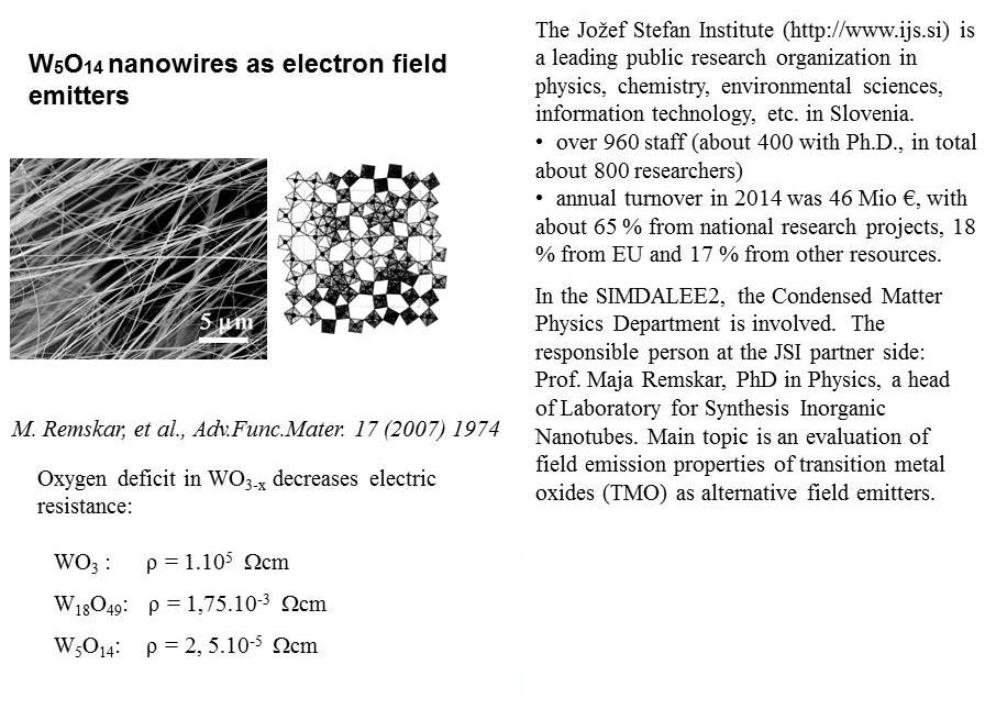
Patents: EP 2 114 827 B1, US 8,496,907 B2, Procedure for the synthesis of threadlike tungsten oxide W5O14.
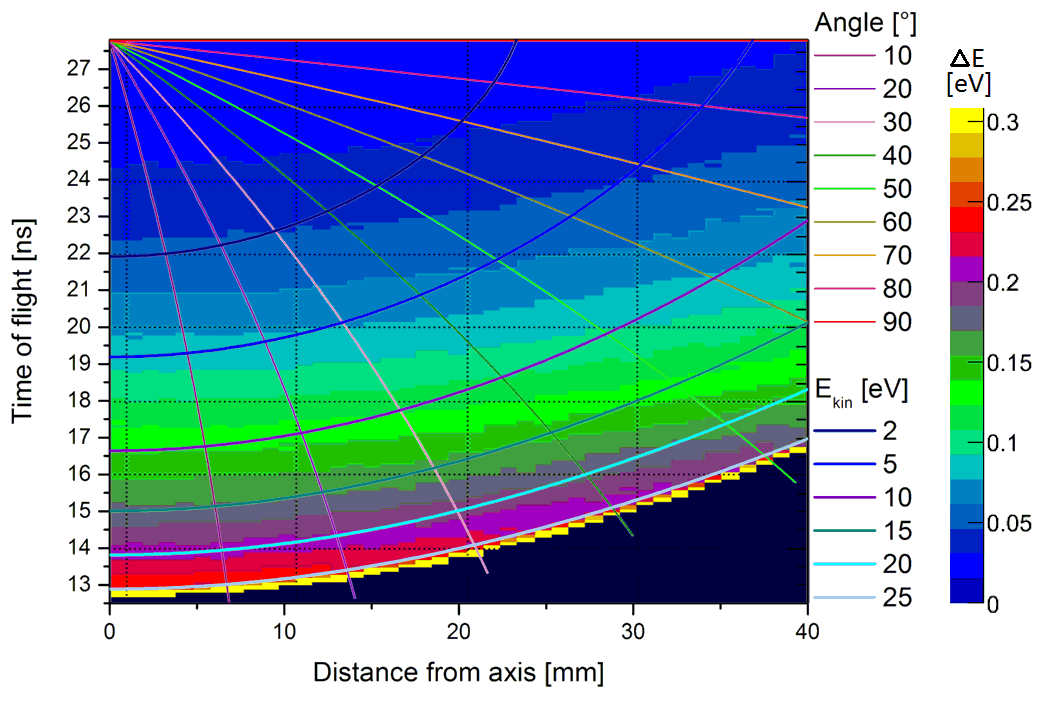
Simulation of cylindrical wide angle time of flight spectrometer. Color encoded is the calculated energy resolution with an estimated error of 0.1 ns flight time and 0.2 mm position read out.
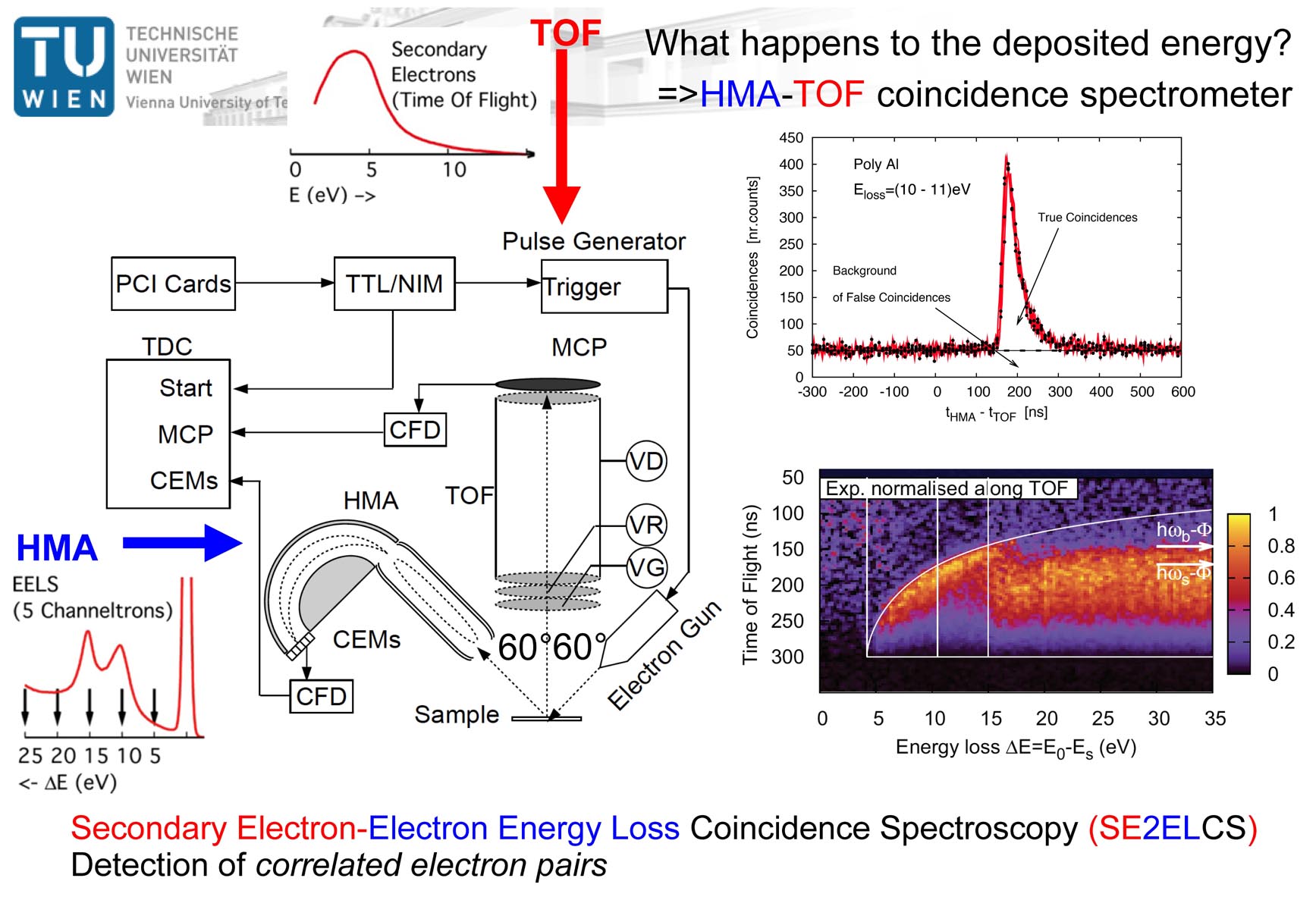
Schematic view of the Secondary Electron–Electron Energy Loss Coincidence Spectrometer apparatus at the TU Vienna. The sharp ridge at energy losses between 5 and 15 eV demonstrating the contribution from Secondary Electrons created in vacuum [see Phys. Rev. B 88, 201407(R) (2013)]
Left: prototype of the simulated wide angle spectrometer for low energy electrons made from Cu-electrodes (5 cm long, ID 10 cm, OD 14 cm). He-cryostat (center) and Pb[111] crystal on Cu-wedge sample transfer system (right).
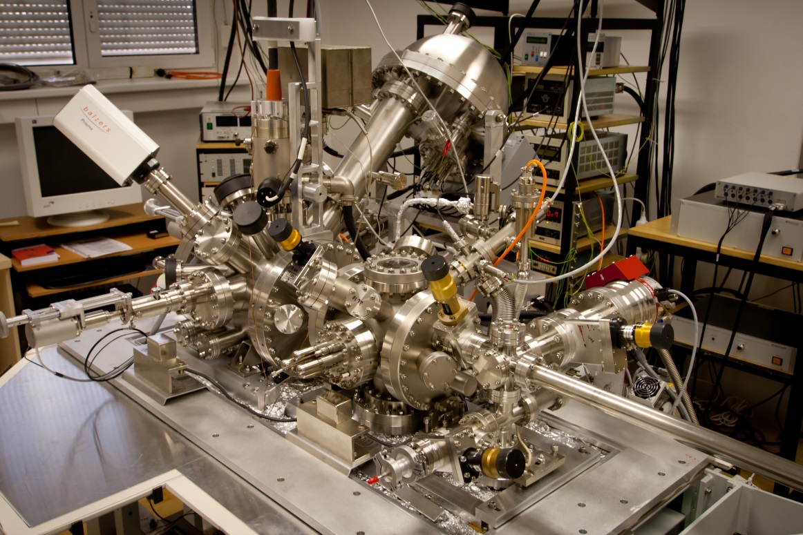
The Phi Scanning Auger Microscope features a Cylindrical Mirror Analyser, Field emission gun, Ar ion gun and rapid sample transfer mechanism.
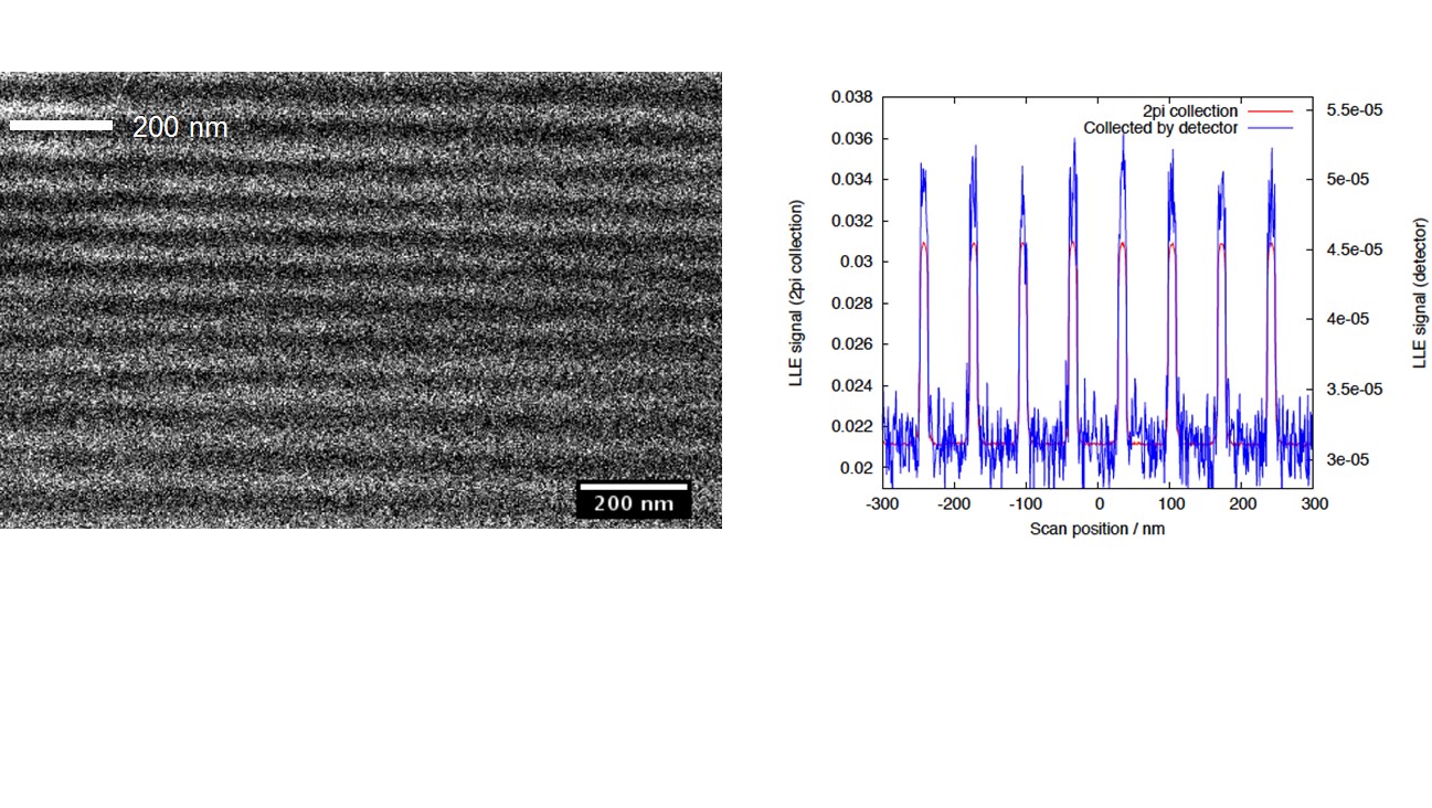
Compositional imaging of a Si0.85Ge0.15 superlattice using the low-loss electron signal (50 eV loss window) in a scanning electron microscope (left). Simulations show improved spatial resolution compared to imaging using the backscattered electron signal (right).
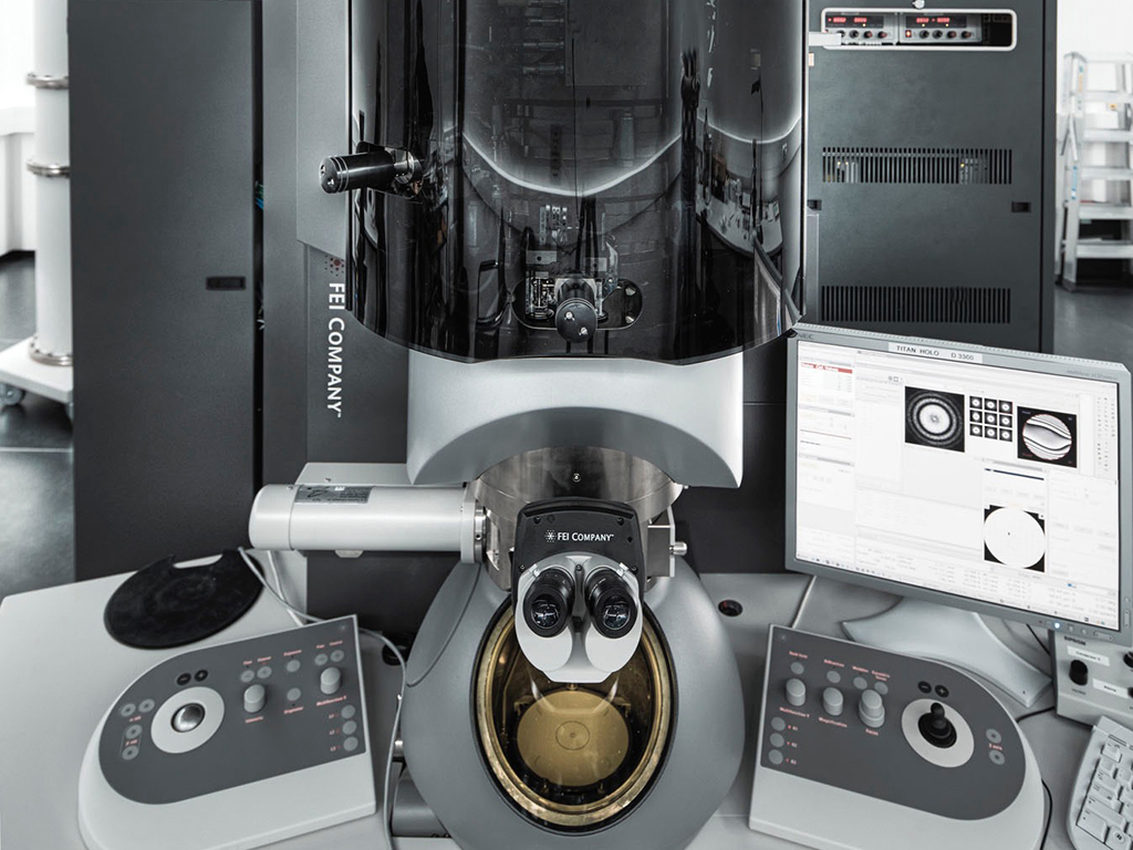
Transmission electron microscope dedicated to off-axis electron holography in Forschungszentrum Jülich
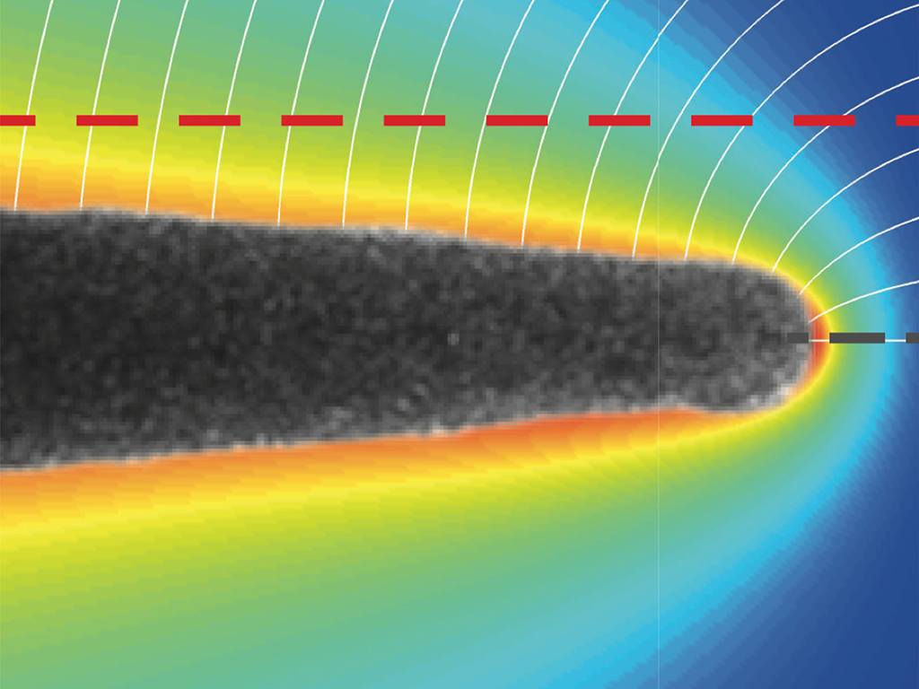
Electric field lines (white) and equipotential contours (colours) measured using electron holography from an electrically biased Fe needle
In either SEM or NFESEM (see diagram) the emitter tip radius has now reached the nm-scale e.g. R=1-5nm when the traditional FN theory –valid for planar surfaces- is not valid anymore.
For R>5nm Kyritsakis and Xanthakis have produced a theory which gives a better tunneling probability and hence current.
For R<5nm one has to start from the beginning i.e. the Schroedinger equation has to be solved taking into account the specific geometry of an emitter tip. Currently, we are working on the solution of both the Laplace and Schroedinger equations in curvilinear coordinates and in particular parabolic coordinates.